Welcome!


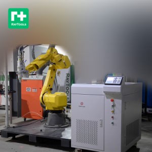
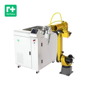
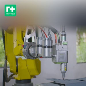
Continuous Laser Welding Portable Fiber Laser Welding Machine Handheld for Aluminum
Product Description
Laser welding has been widely used in the electronics industry, especially in the microelectronics industry. Due to the small heat affected zone, rapid heating concentration, and low thermal stress of laser welding, it has shown unique advantages in the packaging of integrated circuits and semiconductor device shells. In the development of vacuum devices, laser welding has also been applied, such as molybdenum focusing electrodes and stainless steel support rings, fast heating cathode filament components, etc. The thickness of elastic thin-walled corrugated sheets in sensors or temperature controllers ranges from 0.05 to 0.1mm, which is difficult to solve using traditional welding methods. TIG welding is easy to weld through, has poor plasma stability, and has many influencing factors. However, laser welding has a good effect and has been widely used.

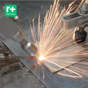
Laser welding is the use of high-energy laser pulses to locally heat a material in a small area. The energy radiated by the laser is directed through heat transfer to the internal diffusion of the material, melting the material and forming a specific molten pool. It is a new type of welding method mainly aimed at the welding of thin-walled materials and precision parts, which can achieve spot welding, butt welding, overlap welding, sealing welding, etc. It has a high aspect ratio, small weld width, small heat affected zone, small deformation, fast welding speed, smooth and beautiful weld seam, no need for treatment or simple treatment after welding, high weld quality, no pores, precise control, small focus light point, high positioning accuracy, and easy to achieve automation.


Recommended Products
Recently Viewed
 Factory Sales China Extruded Decorative Stainless Steel Profile 201/304/316 Stainless Steel Channel Steel
 High Quality Sheet Metal Fabrication Aluminum Stainless Steel Laser Cutting Bending Welding Service Made in China
 High Quality 304 Stainless Steel Round Cold/Hot Rolled 201 304 316 321
 Factory Sales Hot Rolled Spring Steel Flat Bar Sup9 Q235 Ss400 A36 Mild Strength Not Stainless Steel Flat
 Wholesale China Extruded Decorative Stainless Steel Profile 201/304/316 Stainless Steel Channel Steel
Contact Us
Raytools Automation (Shanghai) Co., Ltd


