Welcome!

Main products: SiC Ingot Manufacturer ,As cut SiC Wafer Manufacturer,GaN on SiC Epi Wafer Manufacturer,GaN on Si Epi Wafer Manufacturer,SiC on SiC Epi Wafer Manufacturer,SiC Substrate Wafer Supplier,GaN on Sapphire Substrate Wafer Supplier,SiC Crystal Manufacturer,GaN Substrate Supplier


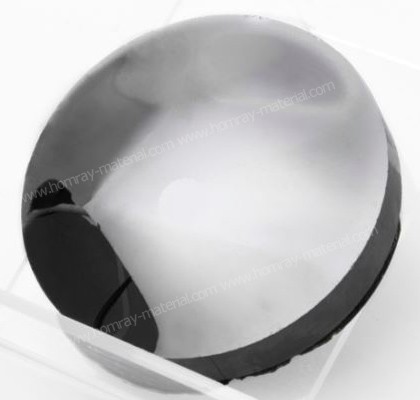
50.8mm 1100um Raw-cut SiC wafer manufacturer 2 inch for grding testing
Basic Info
| Diameter | 2inch | ||||
|---|---|---|---|---|---|
Product Description
50.8mm 1100um Raw-cut SiC wafer manufacturer 2 inch for grding testing
HMT supply 4H-N Conductive type of 2 inch Raw cut SiC wafer with thickness 1100um. The diameter of 2 inch is 50.8mm. We support customized differenct thickness for As-cut SiC wafers. What's As-cut wafer? It means SiC wafer slicing from SiC boule and without grinding and polishing process. Customers can test their grinding or lapping equipment /grinding wheel etc. We always provide high quality but competitive price for SiC produts on the market. please feel free to contact us for quotation and spec.
SiC has high energy conversion efficiency, and will not decrease with the increase of frequency, SiC device operating frequency can reach 10 times of silicon based devices, the same specification of SiC MOSFET total energy loss is only 30% of silicon based IGBT. SiC materials will gradually replace silicon in the fields of high temperature, high frequency and high frequency, and play an important role in 5G communications, aerospace, new energy vehicles and smart power grids.
Recommended Products
Recently Viewed
 50.8mm 1100um Raw-cut SiC wafer manufacturer 2 inch for grding testing
 100mm 4 inch SiC Crystal Boule Supplier For laser cutting
 Raw-cut SiC Wafer Supplier 2 inch unpolished SiC Wafer 1200um
 6 inch As Cut Silicon Carbide Wafer Supplier For SiC diamond grinding
 4 inch unpolished SiC wafer manufacturer with thickness 600um conductive N type
Contact Us
Homray Material Technology

